Theme
Story
Story
세계 1등 기술력만이
반도체 산업을 주도한다
Only World-Leading Technology Leads the Semiconductor Industry
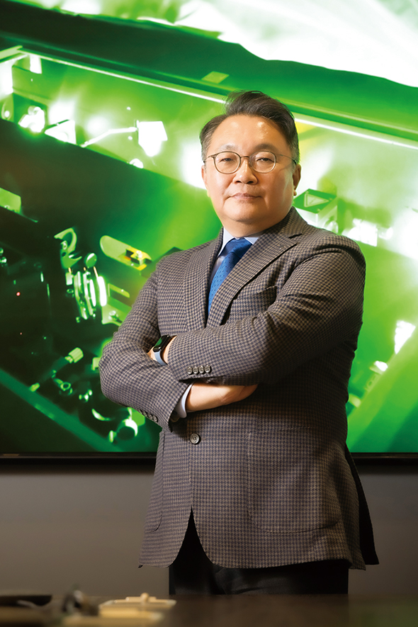
안진호 연구부총장(신소재공학부, CH³IPS 혁신연구센터장, 한양스마트반도체연구원장)
Executive Vice President for Research Affairs Jinho Ahn
(School of Materials Science and Engineering, Director of CH³IPS Innovation Research Center, Director of Hanyang Institute of Smart Semiconductor)
- 글 박영임
- 사진 손초원
- Writing Park Yeong-im
- Photograph Son Cho-won
Scroll Down
최첨단 기술이 구현되는 4차 산업혁명 시대, 미래 기술 선점을 위한 세계의 경쟁이 치열하다. 안진호 연구부총장은 국가 전략산업인 반도체 분야에서 가장 중요한 것이 원천 기술력이라고 강조한다. 치열한 글로벌 시장에서 살아남기 위해서는 세계 1등 기술력을 확보하고, 인공지능을 구성하는 AI 반도체, 차세대 메모리, 첨단 패키징 산업에 집중 투자해야 한다고 역설했다.
In the era of the Fourth Industrial Revolution where cutting-edge technologies are being deployed, global competition is fierce to secure future technologies. Executive Vice President for Research Affairs Jinho Ahn emphasized that fundamental technological capability is the most crucial factor in the semiconductor industry, which is a national strategic industry. He stressed that to survive in the fierce global market, it is essential to secure world-leading technological capabilities and focus investments in AI semiconductors, next-generation memory, and advanced packaging industries that constitute artificial intelligence.
영원한 강자는 없다
지난 1월, 글로벌 기업 및 연구자들이 최첨단 기술을 선보이는 세계 최대, 최고 ICT 박람회 ‘2025 CES’가 열렸다. 기조연설자로 나선 엔비디아의 창업자이자 CEO 젠슨 황의 입에 전 세계 많은 이들의 이목이 쏠렸다. 현재 AI를 활용해 비즈니스 모델을 구축하려면 엔비디아의 GPU가 없어서는 안 되기 때문이다. 젠슨 황 CEO는 이 자리에서 한층 더 향상된 최신 GPU를 소개했다. GPU는 원래 게임용으로 개발된 그래픽 프로세서였는데 강력한 병렬 연산 성능으로 AI 연산, 데이터 분석 등의 고속 연산에 활용되게 됐다. 특히 2022년 말 오픈AI가 선보인 챗GPT에 엔비디아의 GPU가 쓰인 것으로 알려지면서 몸값이 천정부지로 뛰었다. 이렇게 AI 열풍의 최대 수혜자가 된 엔비디아와 극명하게 운명이 갈린 기업이 과거 PC 및 서버용 CPU로 반도체 시장을 주름잡았던 인텔이다. 인텔은 스마트폰, AI라는 신규 반도체 시장 수요에 기술 혁신으로 부응하지 못해 경쟁사에 왕좌를 내주고 말았다.
“한동안 비메모리 반도체에서 인텔이 주도했던 CPU는 가장 큰 영향력을 행사하는 반도체 기술이었습니다. 하지만 최근 엔비디아 GPU의 활용도가 높아지면서 CPU보다 GPU가 중요해져 반도체 산업구도가 바뀌었습니다. 1등 업체일수록 연구개발에 투자를 집중해야 합니다. 자칫 판단을 잘못하거나 기술 개발이 늦어지면 언제든 도태될 수 있죠. 반도체 산업에서 절대 강자란 있을 수 없습니다.”
안진호 연구부총장은 AI 등장과 함께 발 빠르게 그에 맞는 반도체 기술 개발에 돌입한 기업이 시장을 주도하고 있다고 덧붙였다. 기술력 격차가 업체들의 경쟁 구도에 균열을 일으키고 있는 것은 메모리 반도체 시장에서도 마찬가지다. 비메모리 반도체가 아무리 연산력이 뛰어나더라도, 현재의 컴퓨터 구조에서는 메모리 반도체가 방대한 양의 데이터를 빠르고 효율적으로 읽고 처리할 수 있어야 한다. 그래서 기존 D램의 속도와 용량을 키운 HBM(High Bandwidth Memory, 고대역폭 메모리)이 각광받고 있는 것이다.
“HBM은 차선을 늘린 고속도로라 할 수 있습니다. 현재 메모리 반도체 분야에서는 HBM 기술이 뜨거운 감자라 할 수 있죠. SK하이닉스의 HBM 기술이 삼성을 앞지르면서 메모리 반도체 시장의 판도가 바뀌고 있습니다. 하지만 치열한 기술 경쟁 속에서 누구도 안심할 수 없습니다. 상변화 메모리(플래시 메모리의 비휘발성과 램의 속도를 모두 가지고 있는 메모리), M램(자성 메모리) 등 차세대 메모리 반도체에 대한 연구가 활발히 진행되고 있습니다. D램과 낸드 플래시가 한계에 달하면 언제든 이러한 차세대 메모리 반도체가 시장을 차지할 수 있습니다.”
No Champions Are Eternal
Last January, “2025 CES” the world's largest and most prestigious Information and Communications Technology (ICT) exhibition where global companies and researchers showcase cutting-edge technologies, was held. All eyes around the world were on NVIDIA's founder and CEO Jensen Huang, who took the stage as the keynote speaker. This is because NVIDIA's GPUs are now essential for building business models utilizing AI. At this event, CEO Jensen Huang introduced the latest GPU with enhanced capabilities. A graphics processing unit (GPU), originally developed as a graphics processor for gaming, has come to be utilized for high-speed computing such as AI computations and data analysis due to its powerful parallel processing capabilities. Particularly, when it was revealed that NVIDIA's GPUs were used in ChatGPT, introduced by OpenAI in late 2022, their market value skyrocketed. Intel, which once dominated the semiconductor market with PC and server CPUs, has experienced a drastically different fate compared to NVIDIA, which has become the biggest beneficiary of the AI boom. Intel was dethroned by competitors as it failed to respond with technological innovation to new semiconductor market demands in smartphones and AI.
“For a while, Intel CPUs, which led in non-memory semiconductors, were the most influential semiconductor technology. However, as the utilization of NVIDIA GPUs has increased recently, GPUs have become more important than CPUs, changing the structure of the semiconductor industry. The leading companies must focus on investing in research and development. If you make a wrong decision or fall behind in technological development, you can be eliminated at any time. No champions are eternal in the semiconductor industry.”
Executive Vice President for Research Affairs Jinho Ahn added that companies that quickly embarked on developing appropriate semiconductor technology with the emergence of AI are now leading the market. The technological gap is also causing disruptions in the competitive landscape among companies in the memory semiconductor market. No matter how superior the computing power of non-memory semiconductors may be, in current computer architecture, memory semiconductors must be able to read and process vast amounts of data quickly and efficiently. That's why a high bandwidth memory (HBM), which increases the speed and capacity of conventional DRAM, is gaining prominence.
“You can say that HBM is a kind of highway with increased lanes. In the current memory semiconductor field, HBM technology is currently a hot issue. As SK Hynix's HBM technology surpassed Samsung, the landscape of the memory semiconductor market is changing. However, in the midst of fierce technological competition, no one is safe. Research is actively being conducted on next-generation memory semiconductors such as phase-change memory (PCM, a memory that combines both the non-volatility of flash memory and the speed of RAM) and MRAM (magnetic memory). When DRAM and NAND Flash reach their limits, these next-generation memory semiconductors could take over the market at any time.”
소리 없는 총성이 오가는 글로벌 반도체 기술전 속에서 한양대는 ‘한양스마트반도체연구원’과 ‘CH³IPS 혁신연구센터’를 운영하며 국내 반도체 산업 발전에 기여하고 있다.
Amid the silent yet intense global semiconductor technology competition, Hanyang University operates the “Hanyang Institute of Smart Semiconductor” and the “CH³IPS Innovation Research Center,” contributing to the advancement of the domestic semiconductor industry.
반도체 기업 기술 혁신의 산실
소리 없는 총성이 오가는 글로벌 반도체 기술전 속에서 한양대학교도 국내 반도체 산업의 발전에 기여하고자 ‘한양스마트반도체연구원’과 ‘CH³IPS 혁신연구센터’를 운영하고 있다. 혁신연구센터(IRC) 사업은 2023년부터 과학기술정보통신부가 추진하는 집단연구사업으로, 12대 전략산업 분야별로 한 개 대학을 선정해 10년간 500억 원을 지원하는 사업이다. 반도체 분야에서는 한양대 컨소시엄이 선정돼 반도체 기술의 한계를 뛰어넘는 것을 목표로 초미세·고성능·이종집적 반도체 핵심기술을 연구하고 있다.
“연구센터는 3개의 연구그룹으로 구성돼 있습니다. 초미세 공정그룹은 반도체를 더 미세하게 제조하기 위한 공정과 이에 필요한 신소재를 개발하고, 고성능 소자그룹은 저전력에서도 고성능을 발휘할 수 있는 차세대 반도체 소자를 연구합니다. 마지막 이종집적 그룹은 다양한 반도체 소자를 하나의 패키지로 통합해 다양한 성능을 고효율로 발휘할 수 있는 시스템을 연구하고 있습니다.”
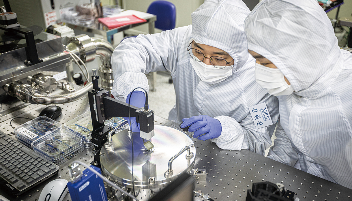
한양스마트반도체연구원은 2022년 한양대가 추진한 융합연구원 육성사업의 일환으로 설립됐다. 동문 기업이자 클린룸 설비 업체인 케이엔솔의 지원을 받아 최첨단 설비를 갖춘 660㎡ 규모의 반도체나노팹을 구축한 바 있다. 이는 반도체 연구 역량을 높여주는 기반이 됐다. 아울러 330㎡ 규모의 패키징팹도 운영 중이다. 이러한 연구 인프라를 구축한 데다 국내 어느 대학보다 많은 수의 연구자를 확보하고 있기에, 한양대가 정부의 혁신연구센터 사업에서 경쟁 대학들을 물리치고 반도체 분야 대상자로 선정될 수 있었다.
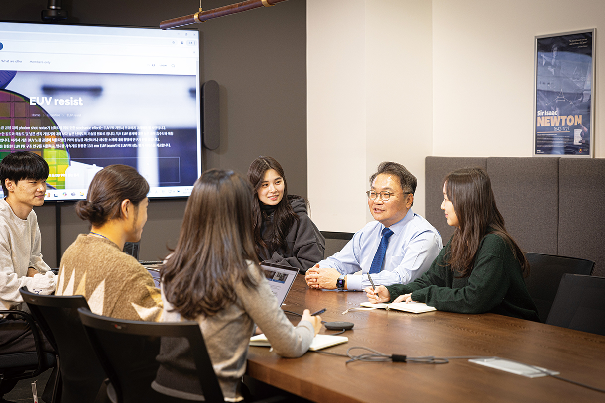
“CH³IPS 혁신연구센터를 1년 넘게 운영하면서 EUV(극자외선) 노광기술을 비롯해 10여 건의 기술을 산업체에 이전했습니다. 혁신연구센터는 단순히 반도체 혁신 기술을 개발하는 데 그치지 않고 반도체 기업들과 협력해 기술 개발 및 인재 양성에도 힘쓰고 있습니다. 이러한 산학협력을 통해 정부 지원이 종료되더라도, 지속가능한 반도체 연구가 이뤄지는 중심지가 되고자 합니다. 이미 60여 개 회원사를 확보해 최신 기술 및 연구 설비를 공유하는 등 산학협력 효과를 높이고 있습니다.”
Cradle of Technological Innovation for Semiconductor Companies
In the midst of the silent but fierce global semiconductor technology warfare, Hanyang University is operating the “Hanyang Institute of Smart Semiconductor (HYISS)” and “CH³IPS Innovation Research Center” to contribute to the development of the domestic semiconductor industry. The Innovation Research Center (IRC) project is a collective research initiative launched by the Ministry of Science and ICT in 2023, which selects one university for each of the 12 strategic industry sectors and provides 50 billion won in support over 10 years. In the semiconductor field, the Hanyang University consortium was selected and is researching the core technologies of ultrafine, high-performance, and heterogeneous integration semiconductors with the goal of surpassing the limitations of current semiconductor technology.
“The IRC consists of three research groups. The ultra-fine process group develops processes and new materials needed to manufacture semiconductors at finer scales, while the high-performance device group researches next-generation semiconductor devices that can deliver high performance even at low power consumption. Finally, the heterogeneous integration group is researching systems that can efficiently demonstrate various performance capabilities by integrating diverse semiconductor devices into a single package.”
The HY-ISS was established in 2022 as part of Hanyang University's convergence research institute development project. With support from K-Ensol, a partner company and cleanroom equipment manufacturer, they have established a 660㎡ semiconductor nano-fab equipped with state-of-the-art facilities. This has become the foundation for enhancing semiconductor research capabilities. Additionally, a packaging fab with an area of 330㎡ is also in operation. Having established such research infrastructure and secured more researchers than any other domestic university, Hanyang University was able to outperform competing universities and be selected as the recipient in the semiconductor field for the government's Innovation Research Center project.
“While operating the CH³IPS Innovation Research Center for over a year, we have transferred more than 10 technologies to industry, including EUV (Extreme Ultraviolet) lithography technology. The Innovation Research Center is not merely developing semiconductor innovation technologies but is also focusing on technology development and talent development in cooperation with semiconductor companies. Through such industry-academic cooperation, we aim to become a hub for sustainable semiconductor research, even after government support ends. With over 60 member companies already secured, we are enhancing industry-academia collaboration effects by sharing cutting-edge technology and research facilities.”

반도체 산업에서 절대 강자란 있을 수 없다. AI 등장에 맞춰 발 빠르게 반도체 기술 개발에 돌입한 기업이 시장을 주도하고 있다
No champions are eternal in the semiconductor industry. Companies that swiftly initiated semiconductor technology development in response to the emergence of AI are leading the market.
반도체 나노 분야 전문가인 안진호 연구부총장은 단순히 반도체 혁신 기술을 개발하는 데 그치지 않고, 반도체 기업들과 협력해 기술 개발 및 인재 양성에도 힘쓰고 있다.
Jinho Ahn, Executive Vice President for Research Affairs and an expert in the field of semiconductor nanotechnology, is not only focused on developing innovative semiconductor technologies but also actively collaborates with semiconductor companies to advance technology development and train talent.
혁신과 도전으로 세계 최고 전문가로 성장
안진호 연구부총장은 지난 30년간 반도체 나노(미세공정) 경쟁의 핵심인 EUV 노광기술에 대한 연구를 진행해 왔다. 특히 EUV-IUCC(EUV-산학협력센터)를 통해 EUV 노광기술 분야 진출을 원하는 국내 반도체 소재·부품·장비(이하 소부장) 기업을 도왔다. 이 모범적인 성과를 인정받아 일본의 수출 규제에 대응해 2021년 반도체 소부장 기업을 육성하는 국가연구협의체(N-Team) 구성 시 롤모델이 되기도 했다.
“국내 반도체 산업은 기형적인 구조를 갖추고 있습니다. 반도체를 제조하는 기술은 세계 최고 수준이지만, 반도체 제조에 필요한 소재, 부품, 장비는 대부분 외국에서 수입해 오고 있습니다. 이제까지는 소부장 기업이 성장하기 어려운 구조였는데, 산업이 탄탄히 성장하기 위해서는 건전한 산업 생태계 조성이 필수적입니다. 기술 개발이 필요한 국내 반도체 업체들이 언제든 믿고 찾아올 수 있는 CH³IPS 혁신연구센터가 되겠습니다.”
반도체 산업 생태계 조정, 발전과 함께 우수한 연구인력을 키워야 한다는 안진호 연구부총장. 그는 한양대의 실용학문 정신을 바탕으로 반도체 관련 공학뿐 아니라 물리학, 화학, 수학 등 자연과학 분야에서도 미래 반도체 산업을 선도할 인재들이 더욱 많이 배출되기를 바란다고 전했다.
“반도체 산업은 끊임없는 혁신과 도전이 필요한 분야입니다. 세계 최고의 전문가가 되려면 전문 분야에서 깊은 지식을 쌓는 것이 중요합니다. 실패를 두려워하지 말고, 새로운 기술을 탐구해 글로벌 시장에서 경쟁할 수 있는 역량을 키워야 합니다. 또한 반도체는 협업과 융합이 중요한 산업입니다. 다양한 분야의 전문가들과 교류하며 폭넓은 시각을 확보하길 바랍니다.”
Becoming a World-Class Expert through Innovation and Challenge
Executive Vice President for Research Affairs Jinho Ahn has been conducting research on EUV lithography technology, which is crucial for semiconductor nano (fine process) competition, for the past 30 years. In particular, through the EUV-IUCC (EUV-Industry University Cooperation Center), he has helped domestic semiconductor materials, parts, and equipment (hereinafter referred to as MPE) companies seeking to enter the field of EUV lithography technology. In recognition of this exemplary achievement, it became a role model for the formation of the National Research Council (N-Team) in 2021, which trains MPE companies in response to Japan's export regulations.
“The domestic semiconductor industry has an imbalanced structure. While our semiconductor manufacturing technology is world-class, most of the materials, parts, and equipment needed for semiconductor manufacturing are imported from foreign countries. Until now, it has been difficult for MPE companies to grow, but creating a healthy industrial ecosystem is essential for solid industry growth. We will become the CH³IPS Innovation Research Center that domestic semiconductor companies can reliably turn to whenever they need technological development.”
Executive Vice President for Research Affairs Jinho Ahn emphasized the need to train outstanding research personnel alongside the adjustment and development of the semiconductor industry ecosystem. Based on Hanyang University's practical academic spirit, he expressed his hope for training more talented individuals who will lead the future semiconductor industry not only in semiconductor-related engineering but also in natural sciences such as physics, chemistry, and mathematics.
“The semiconductor industry is a field that requires constant innovation and challenges. To become a world-class expert, it is crucial to build deep knowledge in your specialized field. Do not fear your failure, but explore new technologies to develop your capabilities to compete in the global market. Furthermore, the semiconductor industry is one where collaboration and convergence are crucial. I hope you will interact with experts from various fields and secure a broad perspective.”